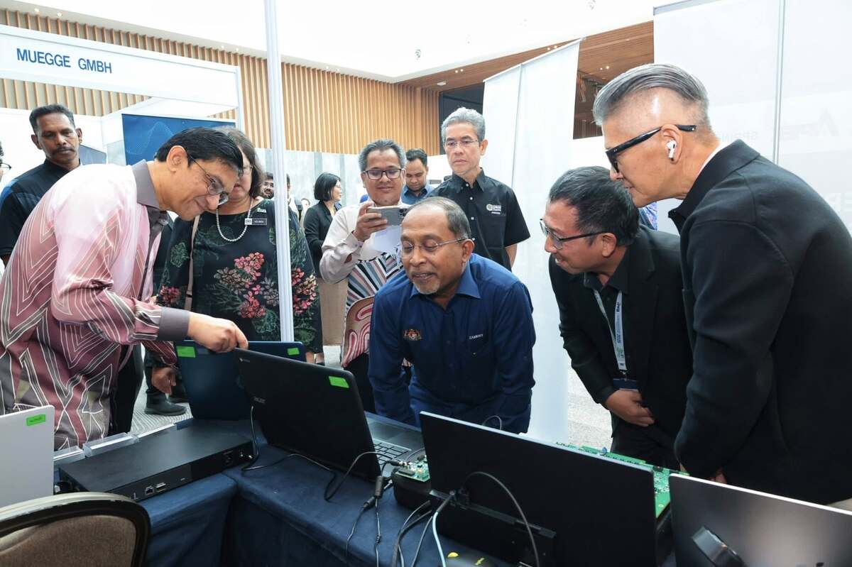
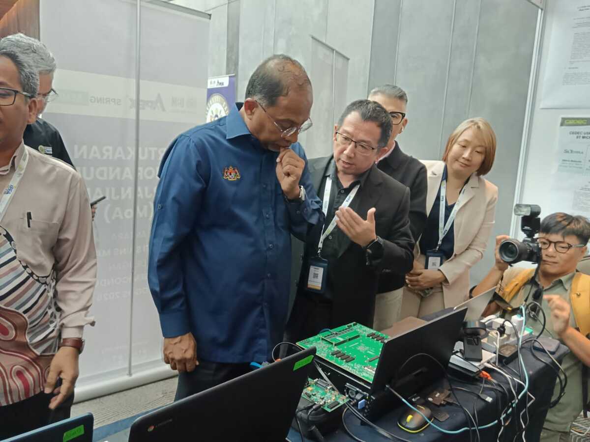
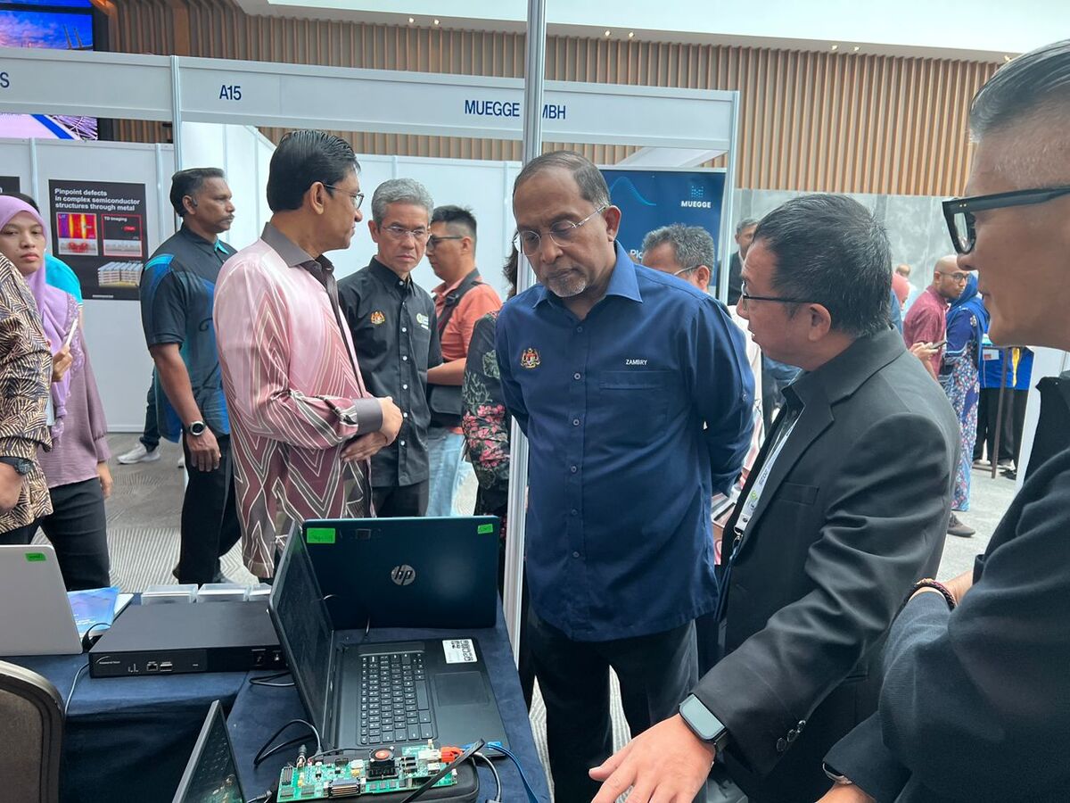
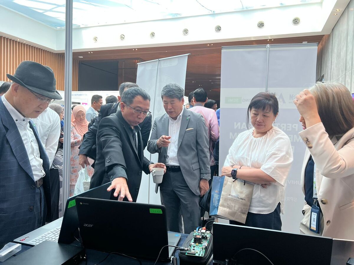
Malaysia’s aspiration to become a regional semiconductor powerhouse hinges on more than factories and funding—it demands mastery of chip design. To achieve this, Spring Semiconductor (SpringSemi) and CEDEC Malaysia have co-developed SpringBlade, the nation’s first SoC prototyping platform, tailored for education, research, and industry acceleration.
SpringBlade is a strategic milestone aligned with the National Semiconductor Strategy (NSS), designed to empower Malaysia’s IC designers, train the next generation of engineers, and prototype world-class silicon systems—from RTL to TSMC tapeout—right here at home.
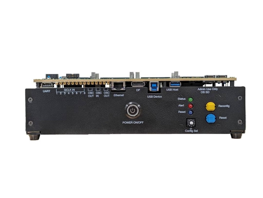
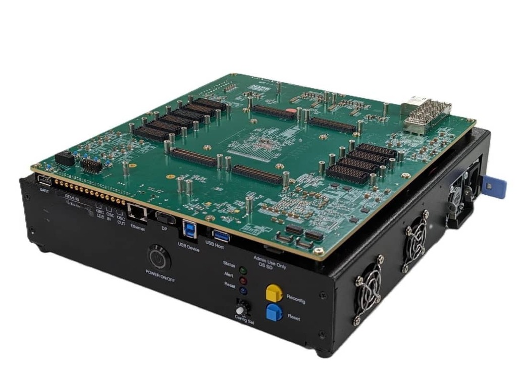
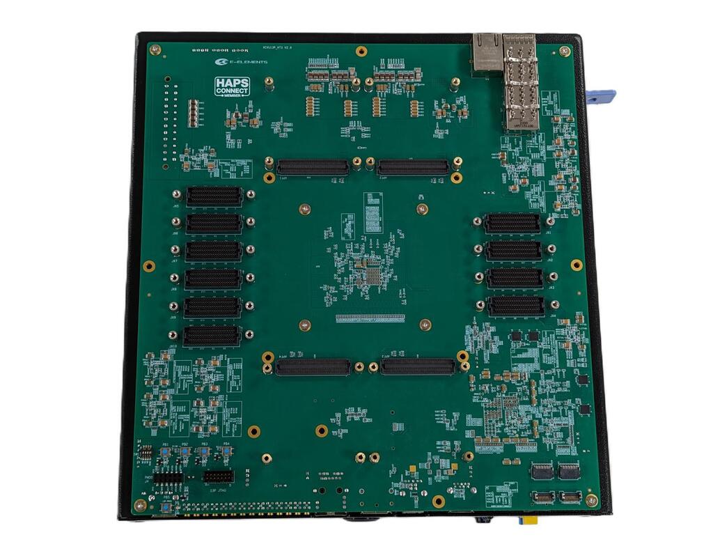
Springblade+ is our inaugural product in this family—built on the robust Xilinx VU13P platform. It marked our first step into merging high-density programmable logic with embedded processing via an add-on ARM Cortex-A53 module. Designed for mid-range complexity, it enabled startups, research teams, and AI developers to rapidly prototype and verify system designs.
Springblade platforms come with integrated remote access through our HaaS Portal, enabling:
Perfect for:
Each Springblade system is compatible with a library of over 50 development modules:
All modules are hot-pluggable, reconfigurable, and supported by a unified SDK.
In 2026, Unleash the next generation of hardware-accelerated design and verification with SpringBlade platforms built on the highest-end UltraScale+ and Versal Premium Adaptive SOCs. Our UltraScale+ VU19P based SpringBlade delivers massive programmable logic with ~9 million system logic cells, 80 high-speed transceivers and over 2,000 I/Os, enabling heavyweight ASIC/SoC emulation, prototyping, networking, and test & measurement workloads with exceptional interconnect and bandwidth.
For cutting-edge heterogeneous acceleration, our Versal Premium VP1502 SpringBlade integrates a powerful blend of 3.76 M logic cells, DSP engines, dual-core Arm® Cortex-A72 application processors, real-time cores, and a rich suite of hardened interfaces for PCIe®, Ethernet, and memory, making it ideal for data-intensive compute, secure network processing, and adaptable system acceleration. At the pinnacle sits our Versal Premium VP1902 SpringBlade — the world’s largest adaptive SoC with ~18.5 million logic cells, up to 160 high-speed SerDes (112 Gbps), extensive DSP and scalar compute, and programmable NoC for unmatched design scalability, debug throughput, and emulation performance.
Contact us to explore how SpringBlades can accelerate your development cycle, boost system performance, and help you conquer even the most demanding embedded, AI, and high-performance computing challenges.

This HaaS model is not just about access, it quietly redraws the map of how hardware gets built. By lowering the barrier to real FPGA infrastructure, Malaysia gains a shared launchpad for semiconductor innovation, connecting design, validation, and future production flows. It creates a natural pathway toward advanced capabilities like hardware security validation, ATE pattern development, and trusted silicon frameworks. Today it is a single node humming in a rack; tomorrow, it becomes the backbone of a nation that treats hardware not as a constraint, but as a canvas.
This platform delivers:
Target users:
*Optional ARM Zyng Card
What this means:


Give us a call! +6012-2180925